
| Version 3 (modified by , 2 years ago) ( diff ) |
|---|
Signal Avoidance Using 5G
WINLAB Summer Internship 2024
Advisors: Dr. Predrag Spasojevic
Group Members: Wesley Chen
Overview
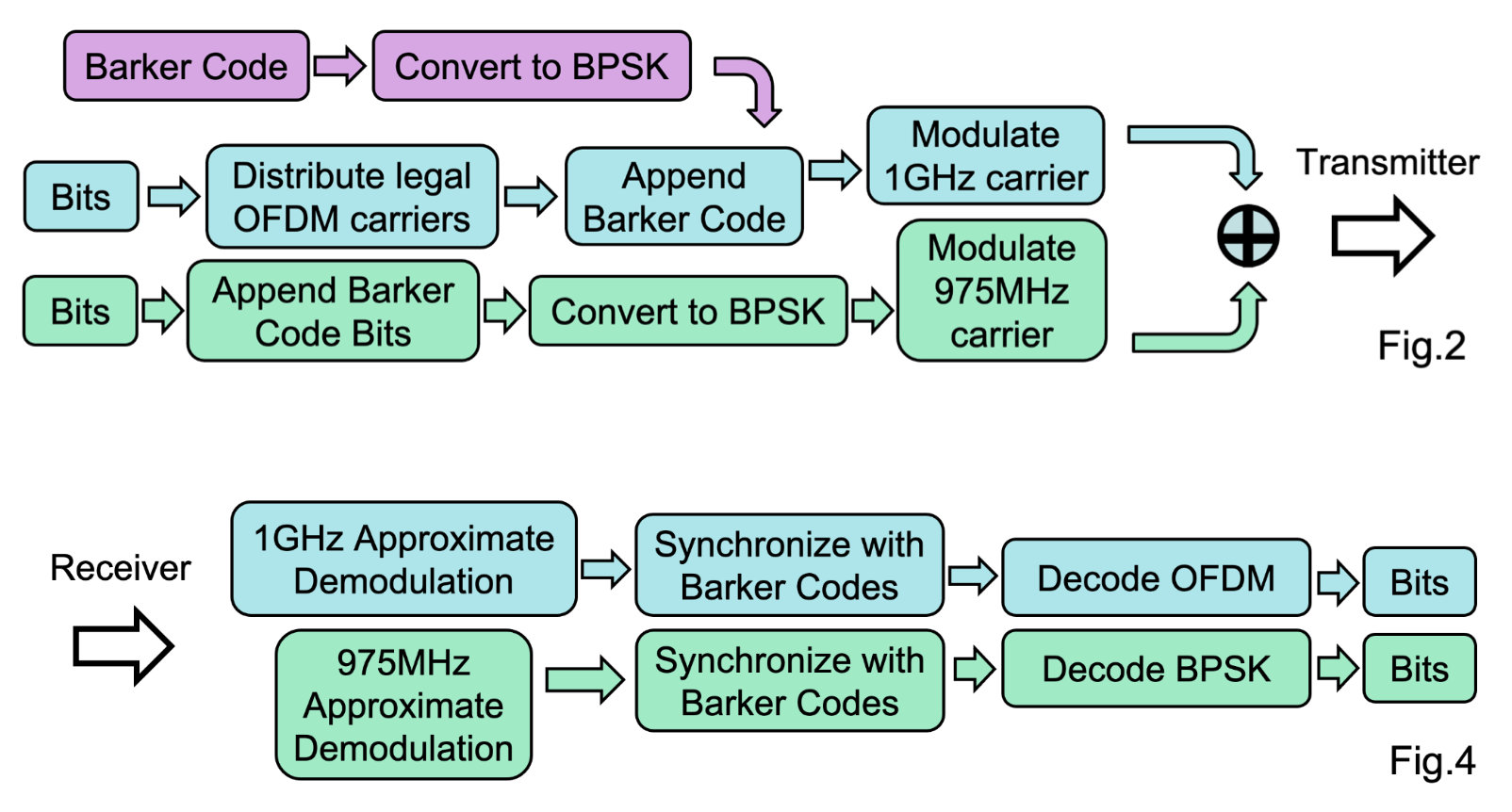
Problem:
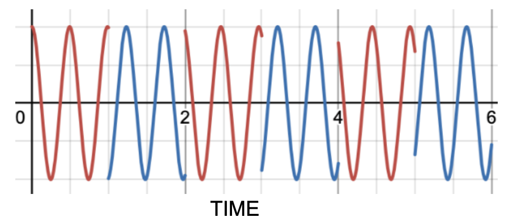
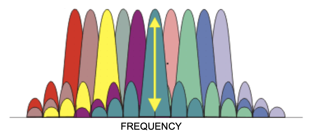
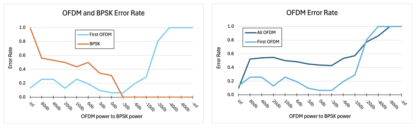
In recent years, there has been a desire to expand the bandwidth of communication standards such as LTE and 5G. However, at many of the bandwidths that are desired to be used, there exist legacy signals that cannot be interfered with. This is made even more difficult by Adjacent Channel Interference (ACI), when signals with very close, but distinct frequencies still impede each other.
Goal:
Build the framework to test signal avoidance.
Devices
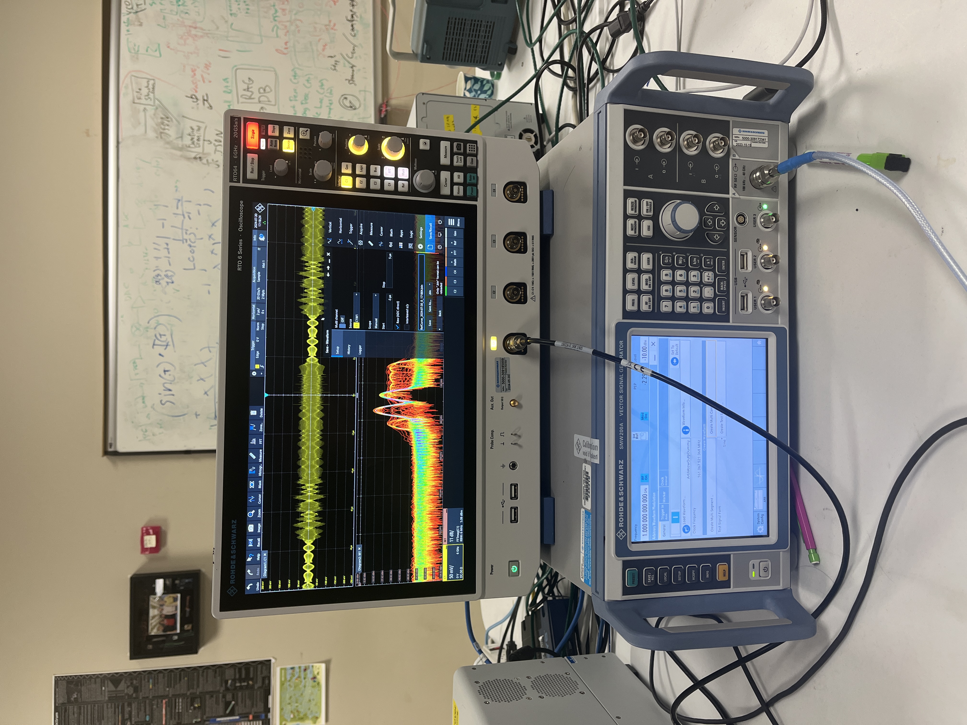
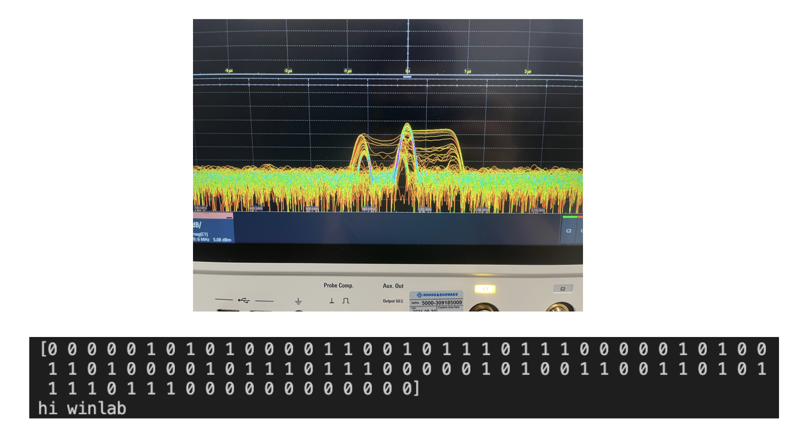
Rhode & Schwarz SMW200A
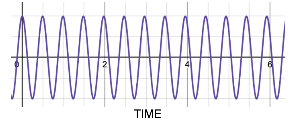
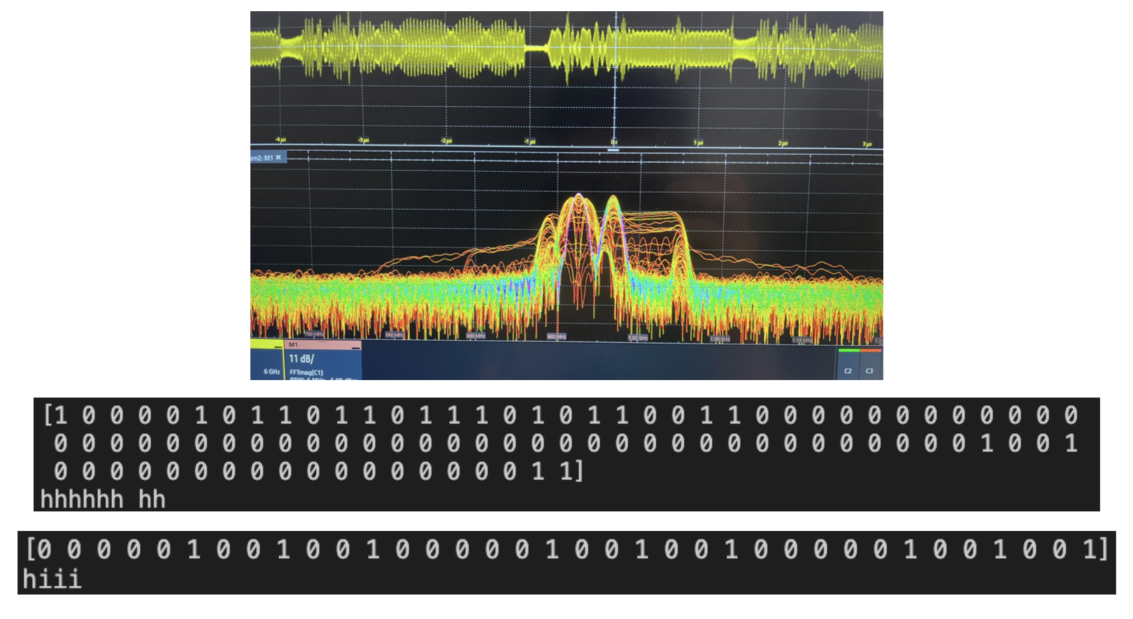
The Rhode & Schwarz SMW200A is a vector signal generator with the ability to output signals from 100kHz to 40GHz with a 50 ohm impedance. The SMW200A has the ability to modulate a carrier signal with an arbitrary waveform (.wv file). For the extent of this project, this waveform was generated in python on a personal computer and uploaded to the machine via the ftp protocol.
Rhode & Schwarz RTO 6 series
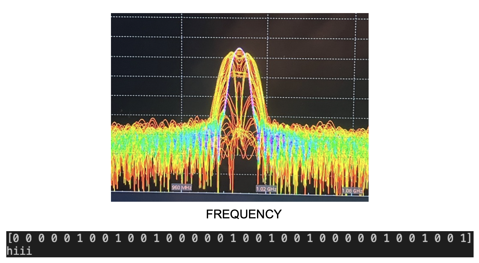
The Rhode & Schwarz RTO 6 series is an oscilloscope with the ability to read signals up to 6GHz and a sample rate of 20 giga-samples per second, although when downloading files from the machine, they are unconverted to 100 giga-samples per second. The RTO has built in mathematical functions such as FFTs to display the frequency domain on the machine. Additionally, as hinted earlier, the RTO can save waveforms in a .csv file which can be downloaded through network (the RTO operates as a windows machine). This file can be analyzed on a personal computer.
everything below this is incomplete and only here for my reference
Week 1
Week 1 PresentationSummary
- Familiarized with breadboard computer components: ICs, logic gates, registers, breadboards, wires, and connectors.
- Learned about fundamental computer components: Fetch-Execute Cycle, CPU, RAM, ALU, and BUS.
- Explored the Fetch-Execute Cycle: Fetch, Decode, Execute.
- Studied the CPU: functions, clock, registers, and ALU.
- Understood RAM: its function, volatility, and direct access capabilities.
- Examined the ALU: performs arithmetic and logical operations.
- Investigated the BUS: facilitates communication between CPU, memory, and peripherals.
- Planned tasks for next week: model and test the ALU using TinkerCad, begin detailed documentation, construct the clock monitor, and build the registers.


Week 2
Week 2 PresentationSummary
- Started and Finished building different components of the clock module
- Started building the A register
- Added more pictures and videos of testing to the documentation
- Tested and troubleshooted problems related to the Clock Module
- First LED wasn't blinking
- Connectivity issues
- Push button wasn't functioning
- Fixed issue due to the different pins on the push button


Week 3
Week 3 PresentationSummary
- Continued and restarted building of the Clock Module
- Used Oscilloscope to reassure connection
- Fixed the push button to be powered by 555 chip
- Technical issue with Blinking LED
- Fixed response delay from Switch
- Finished building the A-Register
- Used 2 74LS173 chips and 1 7LS245 chip
- Started building the Random Access Memory (RAM)
- Used Inverting Chips, Signal Inversion, and Flip-Flop Chips


Attachments (22)
- IMG_3524.JPG (3.3 MB ) - added by 2 years ago.
- Screen Shot 2024-08-06 at 10.32.22 AM.png (104.7 KB ) - added by 2 years ago.
- Screen Shot 2024-08-06 at 10.40.56 AM.png (266.3 KB ) - added by 2 years ago.
- Screen Shot 2024-08-06 at 3.01.41 PM.png (158.0 KB ) - added by 2 years ago.
- Screen Shot 2024-08-06 at 3.01.51 PM.png (191.0 KB ) - added by 2 years ago.
- Screen Shot 2024-08-06 at 2.31.04 PM.png (163.0 KB ) - added by 2 years ago.
- Screen Shot 2024-08-06 at 2.31.18 PM.png (187.7 KB ) - added by 2 years ago.
- Screen Shot 2024-08-06 at 3.02.06 PM.png (144.9 KB ) - added by 2 years ago.
- Screen Shot 2024-08-06 at 3.13.48 PM.png (244.6 KB ) - added by 2 years ago.
- Screen Shot 2024-08-06 at 3.14.10 PM.png (87.7 KB ) - added by 2 years ago.
- Screen Shot 2024-08-06 at 3.14.18 PM.png (275.9 KB ) - added by 2 years ago.
- Screen Shot 2024-08-06 at 3.18.35 PM.png (1.2 MB ) - added by 2 years ago.
- Screen Shot 2024-08-06 at 3.20.03 PM.png (322.4 KB ) - added by 2 years ago.
- Screen Shot 2024-08-06 at 5.44.33 PM.png (266.9 KB ) - added by 2 years ago.
- Screen Shot 2024-08-06 at 5.55.59 PM.png (174.1 KB ) - added by 2 years ago.
- Screen Shot 2024-08-06 at 6.03.54 PM.png (116.4 KB ) - added by 2 years ago.
- Screen Shot 2024-08-06 at 6.04.02 PM.png (60.2 KB ) - added by 2 years ago.
- Screen Shot 2024-08-06 at 6.38.04 PM.png (940.3 KB ) - added by 2 years ago.
- Screen Shot 2024-08-06 at 6.38.11 PM.png (271.8 KB ) - added by 2 years ago.
- Screen Shot 2024-08-06 at 6.38.20 PM.png (373.9 KB ) - added by 2 years ago.
- Screen Shot 2024-08-06 at 6.38.29 PM.png (1.1 MB ) - added by 2 years ago.
- Screen Shot 2024-08-06 at 6.38.38 PM.png (171.0 KB ) - added by 2 years ago.